What makes these chips smart
A look at how we actually make our wafers — from 300mm substrates and advanced packaging to the testing that happens on every single one.
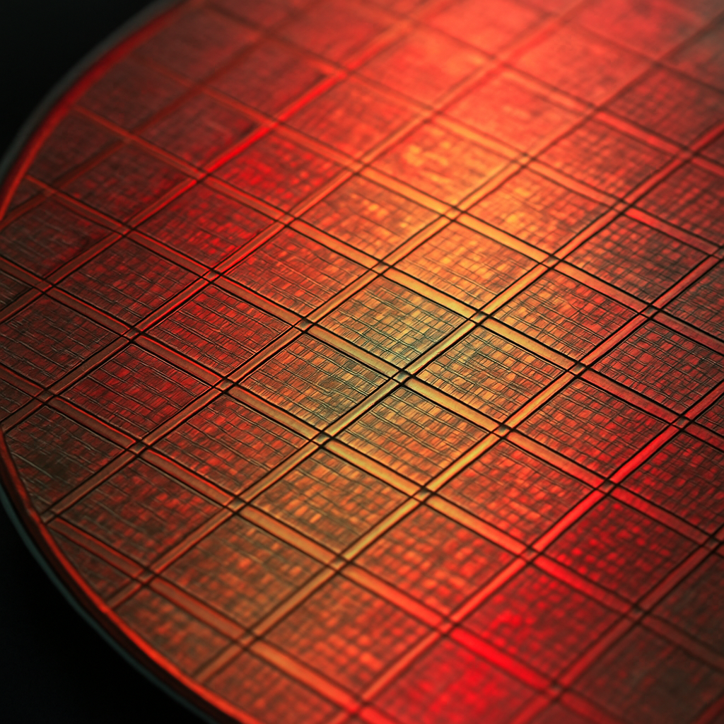
Quantum capability, engineered into silicon
Getting quantum behaviour out of silicon is genuinely hard. The material has to be clean, the interconnects dense, and the tolerances tighter than anything classical chips demand. That is the problem our process is designed around.
Because we only make wafers, we can put all of our attention there — refining a single process until it is dependable enough to build a roadmap on.
From substrate to smart chip
- 01
300mm Quantum Wafers
A pure-play foundry dedicated entirely to producing 300mm quantum wafers — the substrate on which the next generation of quantum hardware is built.
- 02
Through-Silicon Vias (TSV)
Vertical interconnects pass directly through the silicon, enabling dense, high-performance 3D integration that classical packaging cannot match.
- 03
Wafer-Scale Bumping
Advanced bumping across the full wafer delivers the interconnect density and reliability required for production-grade quantum devices.
- 04
In-Line Testing & Characterization
Every wafer is measured throughout fabrication, surfacing the data partners need to refine designs with confidence.
- 05
Process Design Kits (PDKs)
Dedicated PDKs give design teams a head start, accelerating development and dramatically shortening iteration cycles.